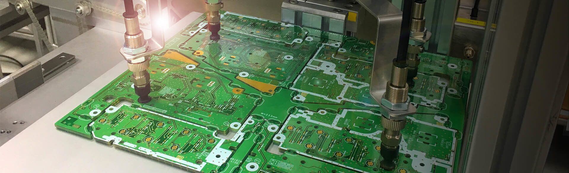
High Density Interconnect PCBs (HDIs) represent a transformative force in the electronics industry, embodying the principles of compactness and power. In a world where electronic devices are constantly evolving and consumer expectations are ever-increasing, HDIs stand as a testament to the art of achieving maximum functionality in minimal space.
The Pursuit of Miniaturization
HDIs are at the forefront of the pursuit of miniaturization. As consumer preferences increasingly favor smaller, sleeker, and more portable devices, HDI PCB fabrication packs an astonishing amount of functionality into compact gadgets. This miniaturization is crucial for industries like wearables, IoT, and aerospace, where space constraints are a critical consideration.
Unleashing Unprecedented Power
Compactness doesn’t mean compromising on power; in fact, HDIs excel in unlocking the full potential of electronic devices. By densely packing components and employing intricate routing, these PCBs enable devices to perform with incredible power and speed. This is particularly vital for emerging technologies like 5G communication, AI, and autonomous vehicles.
Thermal Management: Keeping Cool Under Pressure
As electronic components continue to grow in power, efficient heat management is paramount. HDIs are designed with advanced thermal vias and heat sinks that efficiently dissipate heat, ensuring devices remain reliable and durable under demanding conditions. This capability is invaluable for industries where thermal control is a critical factor.
Design Freedom and Flexibility
HDIs offer unparalleled design freedom and flexibility. Engineers can accommodate components of various shapes and sizes, enabling creative and innovative product designs. This adaptability simplifies the integration of additional features, such as sensors, antennas, and connectors, allowing for the creation of versatile electronic products.
Sustainability in Compactness
As the world embraces sustainability, HDIs contribute by reducing the environmental footprint. Smaller and lighter devices lead to energy-efficient products with a reduced ecological impact. This aligns with the growing global emphasis on sustainable and eco-friendly electronics.
Conclusion
High Density Interconnect PCBs represent the pinnacle of compactness and power in the electronics industry. Their ability to maximize functionality in minimal space, deliver incredible performance, and manage heat efficiently makes them indispensable in an ever-evolving landscape. As consumers continue to seek smaller, more powerful, and environmentally responsible electronic devices, HDIs will continue to be the driving force behind innovation, enabling the creation of cutting-edge technology that shapes the future. In a world where compactness and power are prized attributes, High Density Interconnect PCBs prove that great things can indeed come in small packages.